
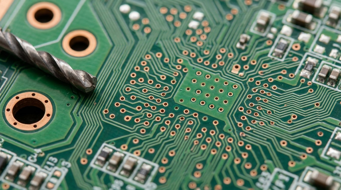
As electronic devices continue to shrink while delivering greater performance, manufacturers need advanced printed circuit board (PCB) solutions. Laser Drilled Microvia Technology has emerged as one of the most important innovations in modern PCB manufacturing. It enables smaller, faster, and more reliable electronic products by creating ultra-small electrical connections between PCB layers.
From smartphones and wearable devices to automotive electronics and aerospace systems, Laser Drilled Microvia Technology plays a crucial role in supporting high-density interconnect (HDI) circuit boards. This article explores how the technology works, its advantages, applications, challenges, and why it has become the preferred choice for advanced electronics.
What Is Laser Drilled Microvia Technology?
Laser Drilled Microvia Technology is a manufacturing process that uses precision laser beams to create microscopic holes, called microvias, in printed circuit boards. These tiny holes establish electrical connections between different PCB layers without requiring large through-holes.
Unlike traditional mechanical drilling, laser drilling produces extremely small vias—often less than 150 micrometers in diameter—with exceptional accuracy. This capability allows engineers to design compact, multilayer circuit boards that support increasingly powerful electronic devices.
How Laser Drilled Microvia Technology Works
The manufacturing process involves several carefully controlled steps:
1. PCB Material Preparation
Manufacturers prepare copper-clad laminates or HDI substrates designed for laser processing.
2. Laser Drilling
High-energy laser beams precisely remove dielectric material to create blind or buried microvias without damaging surrounding layers.
3. Cleaning (Desmear)
After drilling, chemical or plasma cleaning removes residue from the hole walls to improve electrical performance.
4. Copper Plating
Copper is deposited inside each microvia to establish reliable electrical conductivity.
5. Inspection
Automated optical inspection verifies diameter, alignment, taper, and plating quality before final PCB assembly.
Types of Lasers Used
Several laser systems are commonly employed in Laser Drilled Microvia Technology.
CO₂ Lasers
CO₂ lasers offer high drilling speed and cost efficiency for standard HDI boards. They are ideal for many commercial PCB applications.
UV Lasers
Ultraviolet lasers create even smaller microvias with cleaner edges and minimal thermal damage. They can directly process copper and fine-pitch designs.
Picosecond Lasers
Modern picosecond laser systems produce excellent dimensional accuracy while significantly reducing heat-affected zones, making them suitable for advanced semiconductor packaging.
Advantages of Laser Drilled Microvia Technology
Exceptional Precision
Laser drilling achieves hole diameters much smaller than mechanical drilling, supporting increasingly dense PCB layouts.
Higher Circuit Density
Smaller vias allow designers to route more electrical traces within limited board space, enabling miniaturized electronics.
Improved Signal Integrity
Shorter electrical pathways reduce resistance, inductance, and signal loss, improving high-speed data transmission.
Greater Reliability
Laser-drilled microvias experience less mechanical stress than traditional drilled holes, resulting in better long-term durability.
Faster Manufacturing
Automated laser systems drill thousands of microvias rapidly while maintaining consistent quality.
Reduced Material Damage
Properly optimized laser parameters minimize cracking, delamination, and thermal deformation.
Applications of Laser Drilled Microvia Technology
The versatility of Laser Drilled Microvia Technology makes it essential across numerous industries.
Smartphones
Modern smartphones rely on HDI PCBs with laser-drilled microvias to support compact processors, cameras, and wireless communication.
Wearable Devices
Smartwatches and fitness trackers require miniature multilayer boards that maximize functionality while conserving space.
Medical Electronics
Medical imaging systems, implantable devices, and portable diagnostic equipment benefit from the technology’s precision and reliability.
Automotive Electronics
Advanced driver assistance systems (ADAS), electric vehicles, battery management systems, and infotainment modules use HDI circuit boards manufactured with laser-drilled microvias.
Aerospace and Defense
Mission-critical electronics require durable interconnections capable of performing under harsh environmental conditions.
Data Centers and Networking
High-speed networking equipment depends on compact PCB architectures that maintain signal integrity at increasingly higher frequencies.
Laser Drilled Microvia Technology vs. Mechanical Drilling
| Feature | Laser Drilled Microvia Technology | Mechanical Drilling |
| Hole Size | Extremely small | Larger diameter |
| Precision | Very high | Moderate |
| Blind Vias | Easily created | Limited capability |
| HDI Compatibility | Excellent | Limited |
| Tool Wear | None | Drill bits wear over time |
| Production Speed | High automation | Slower for microvias |
| Cost for Fine Features | More efficient | Higher tooling costs |
Mechanical drilling remains useful for larger through-holes, but Laser Drilled Microvia Technology dominates advanced HDI manufacturing because it supports smaller features with greater consistency.
Design Considerations
Engineers should consider several factors when implementing Laser Drilled Microvia Technology.
- Maintain proper aspect ratios for reliable plating.
- Select compatible laminate materials.
- Optimize via placement for thermal management.
- Ensure sufficient copper thickness.
- Follow manufacturer design rules for stacked and staggered microvias.
- Plan inspection and testing throughout production.
Careful design improves yield while reducing manufacturing costs.
Manufacturing Challenges
Despite its many benefits, Laser Drilled Microvia Technology presents several challenges.
Equipment Investment
Industrial laser drilling systems require substantial capital investment.
Process Optimization
Laser power, pulse duration, wavelength, and scanning speed must be carefully adjusted for each substrate.
Material Compatibility
Different PCB materials respond differently to laser energy, requiring customized process settings.
Quality Control
Manufacturers continuously monitor taper angle, roundness, debris, and plating quality to ensure long-term reliability.
Future Trends in Laser Drilled Microvia Technology
The future of Laser Drilled Microvia Technology is closely tied to advances in electronics manufacturing.
Emerging trends include:
- Ultra-fast picosecond and femtosecond laser systems.
- Artificial intelligence for process optimization.
- Smaller sub-10 µm microvias.
- Improved environmentally friendly drilling methods.
- Greater adoption in 2.5D and 3D semiconductor packaging.
- Higher automation using smart manufacturing systems.
As semiconductor packaging continues evolving, laser drilling capabilities will become even more sophisticated.
Why Manufacturers Prefer Laser Drilled Microvia Technology
Manufacturers increasingly choose Laser Drilled Microvia Technology because it provides:
- Higher production efficiency.
- Superior electrical performance.
- Better manufacturing consistency.
- Increased design flexibility.
- Reduced PCB size.
- Greater reliability.
- Support for next-generation electronic devices.
These advantages make it the preferred solution for companies producing advanced HDI printed circuit boards.
Conclusion
Laser Drilled Microvia Technology has transformed modern PCB manufacturing by enabling compact, reliable, and high-performance electronic products. Its unmatched precision, support for high-density interconnects, and ability to create ultra-small blind microvias make it indispensable across industries ranging from consumer electronics to aerospace.
As demand for smaller, faster, and more powerful devices continues to grow, Laser Drilled Microvia Technology will remain at the forefront of PCB innovation. Ongoing improvements in laser systems, automation, and materials science promise even greater manufacturing accuracy, improved yields, and expanded applications in the years ahead. With continuous technological advancements, this cutting-edge manufacturing process will continue shaping the future of electronic design and production.